 | –≠–ª–µ–∫—Ç—Ä–æ–Ω–Ω—ã–π –∫–æ–º–ø–æ–Ω–µ–Ω—Ç: LAN83C180 | –°–∫–∞—á–∞—Ç—å:  PDF PDF  ZIP ZIP |

SMSC DS ≠ LAN83C180
Rev. 08/24/2001
LAN83C180
PRELIMINARY
10/100 Fast Ethernet PHY Transceiver
FEATURES
Single Chip 100Base-TX/10Base-T Ethernet
Physical Layer (PHY) Solution
Dual Speed ≠ 10/100 Mbps
Full MII Interface for a Glueless MAC Connection
MI Interface for Configuration and Status
Half Duplex and Full Duplex in Both 10BASE-T and
100BASE-TX
Repeater
Mode
Extended Register Set
Integrated 10BASE-T Transceivers and
Receive/Transmit Filters
Integrated Adaptive Equalizer and Base Line
Wander Correction
Full Auto Negotiation Support for 10BASE-T and
100BASE-TX Both Half and Full Duplex
Parallel Detection for Supporting Non Auto
Negotiation Legacy in Link Partners
Low
Current
Low Power Mode
Internal Power on Reset
Single Magnetics for 10BASE-T and 100BASE-TX
Operation for a Single RJ45 Connector
Support for IEEE-802.3x Flow Control Specification
5 Integrated Status LED Drivers
-
Full
Duplex
-
10/100
-
Activity
-
Collision
-
Link
Low External Component Count
64 Pin TQFP Package (1.0 mm Body Thickness)
GENERAL DESCRIPTION
The LAN83C180 is a single chip CMOS physical layer (PHY) solution providing all necessary functions between the
Media Independent Interface (MII) and the magnetics connected to Category 5 twisted pair media. It is designed for
10BASE-T and 100BASE-TX Ethernet, and is based on the IEEE 802.3 specifications.
The LAN83C180 is compatible with the Auto Negotiation section of IEEE 802.3u and provides all the support needed
for the IEEE 802.3x Full Duplex specification. The LAN83C180 can operate in adapter mode or repeater/switch
modes.
ORDERING INFORMATION
Order Number: LAN83C180 TQFP
64 Pin TQFP Package

SMSC DS ≠ LAN83C180
Page 2
Rev. 08/24/2001
© 2000 STANDARD MICROSYSTEMS CORPORATION (SMSC)
80 Arkay Drive
Hauppauge, NY 11788
(631) 435-6000
FAX (631) 273-3123
Standard Microsystems is a registered trademark of Standard Microsystems Corporation, and SMSC is a trademark of Standard Microsystems
Corporation. Product names and company names are the trademarks of their respective holders. Circuit diagrams utilizing SMSC products are included
as a means of illustrating typical applications; consequently complete information sufficient for construction purposes is not necessarily given. Although
the information has been checked and is believed to be accurate, no responsibility is assumed for inaccuracies. SMSC reserves the right to make
changes to specifications and product descriptions at any time without notice. Contact your local SMSC sales office to obtain the latest specifications
before placing your product order. The provision of this information does not convey to the purchaser of the semiconductor devices described any
licenses under the patent rights of SMSC or others. All sales are expressly conditional on your agreement to the terms and conditions of the most
recently dated version of SMSC's standard Terms of Sale Agreement dated before the date of your order (the "Terms of Sale Agreement"). The product
may contain design defects or errors known as anomalies which may cause the product's functions to deviate from published specifications. Anomaly
sheets are available upon request. SMSC products are not designed, intended, authorized or warranted for use in any life support or other application
where product failure could cause or contribute to personal injury or severe property damage. Any and all such uses without prior written approval of an
Officer of SMSC and further testing and/or modification will be fully at the risk of the customer. Copies of this document or other SMSC literature, as well
as the Terms of Sale Agreement, may be obtained by visiting SMSC's website at http://www.smsc.com.
SMSC DISCLAIMS AND EXCLUDES ANY AND ALL WARRANTIES, INCLUDING WITHOUT LIMITATION ANY AND ALL IMPLIED WARRANTIES
OF MERCHANTABILITY, FITNESS FOR A PARTICULAR PURPOSE, TITLE, AND AGAINST INFRINGEMENT, AND ANY AND ALL WARRANTIES
ARISING FROM ANY COURSE OF DEALING OR USAGE OF TRADE.
IN NO EVENT SHALL SMSC BE LIABLE FOR ANY DIRECT, INCIDENTAL, INDIRECT, SPECIAL, PUNITIVE, OR CONSEQUENTIAL DAMAGES;
OR FOR LOST DATA, PROFITS, SAVINGS OR REVENUES OF ANY KIND; REGARDLESS OF THE FORM OF ACTION, WHETHER BASED ON
CONTRACT; TORT; NEGLIGENCE OF SMSC OR OTHERS; STRICT LIABILITY; BREACH OF WARRANTY; OR OTHERWISE; WHETHER OR
NOT ANY REMEDY IS HELD TO HAVE FAILED OF ITS ESSENTIAL PURPOSE, AND WHETHER OR NOT SMSC HAS BEEN ADVISED OF THE
POSSIBILITY OF SUCH DAMAGES.

SMSC DS ≠ LAN83C180
Page 3
Rev. 08/24/2001
TABLE OF CONTENTS
FEATURES ................................................................................................................................................................... 1
GENERAL DESCRIPTION............................................................................................................................................ 1
PIN CONFIGURATION ................................................................................................................................................. 4
DESCRIPTION OF PIN FUNCTIONS ........................................................................................................................... 5
FUNCTIONAL DESCRIPTION...................................................................................................................................... 7
25MHz Reference Clock ............................................................................................................................................ 7
10BASE-T OPERATION ............................................................................................................................................... 7
10Mb/s Data Transfer on the MII ............................................................................................................................... 7
RX10 Clock Recovery................................................................................................................................................ 7
100MHz Synthesizer.................................................................................................................................................. 7
TX10 Pulse Shaper & Filter ....................................................................................................................................... 7
TX10 Latency............................................................................................................................................................. 7
RX10 Filter & RX10 Signal Detect ............................................................................................................................. 7
RX10 Latency ............................................................................................................................................................ 8
100BASE-TX OPERATION........................................................................................................................................... 8
100Mb/s Data Exchange on the MII Interface............................................................................................................ 8
125MHz Synthesizer.................................................................................................................................................. 8
TX100 PISO, Encoder and Scrambler ....................................................................................................................... 8
TX100 Driver.............................................................................................................................................................. 8
TX100 Latency........................................................................................................................................................... 8
RX100 Equalizer & Base-line Wander Correction ..................................................................................................... 8
RX100 Clock Recovery.............................................................................................................................................. 8
RX100 SIPO, Decoder and Descrambler .................................................................................................................. 9
RX100 Latency .......................................................................................................................................................... 9
100Mb/s Transmit Errors ........................................................................................................................................... 9
100Mb/s Receive Errors ............................................................................................................................................ 9
CONTROLS ................................................................................................................................................................ 10
Initialization (nRESET)............................................................................................................................................. 10
Reset Mode ............................................................................................................................................................. 10
Low-Power Mode ..................................................................................................................................................... 10
Loopback Mode ....................................................................................................................................................... 10
Repeater Mode ........................................................................................................................................................ 10
ICFG - Interrupt........................................................................................................................................................ 11
Auto-Negotiation Enable (ANEN)............................................................................................................................. 11
MII Management Interface ....................................................................................................................................... 11
MANAGEMENT .......................................................................................................................................................... 13
MAC Access to PHY Management Registers .......................................................................................................... 13
RESISTER SET ....................................................................................................................................................... 13
OPERATING CONDITIONS........................................................................................................................................ 18
MAXIMUM GUARANTEED RATINGS*.................................................................................................................... 18
DC ELECTRICAL CHARACTERISTICS .................................................................................................................. 18
DIFFERENTIAL OUTPUT........................................................................................................................................ 18
AC ELECTRICAL CHARACTERISTICS .................................................................................................................. 19
REFCLK................................................................................................................................................................... 19
RX_CLK................................................................................................................................................................... 19
TX_CLK ................................................................................................................................................................... 19
MDC......................................................................................................................................................................... 19
EXTERNAL COMPONENTS....................................................................................................................................... 20
Connecting an External 25MHz Reference.............................................................................................................. 20
nRESET Pull-up Resistor......................................................................................................................................... 20
RX Input Decoupling................................................................................................................................................ 20
Crystal Oscillator...................................................................................................................................................... 20
PACKAGE DETAILS .................................................................................................................................................. 21
LAN83C180 REVISIONS ............................................................................................................................................ 22
SMSC DS ≠ LAN83C180
Page 4
Rev. 08/24/2001
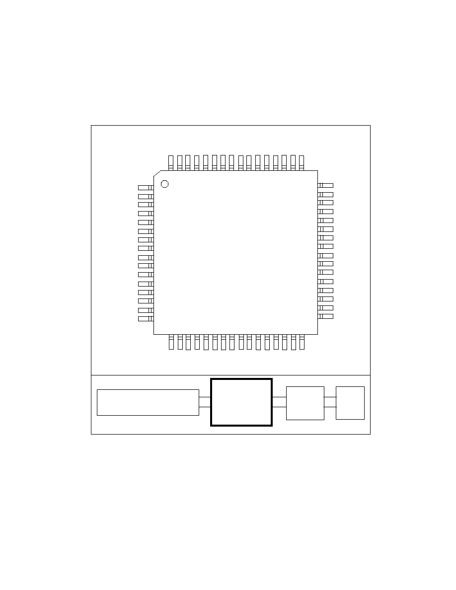
PIN CONFIGURATION
FIGURE 1 ≠ SYSTEM BLOCK DIAGRAM
RXGND1
RX
I
P
RXI
N
R
X
VDD1
RPTR
AN
E
N
IC
F
G
T
X
VDD1
TX
ON
TX
O
P
T
X
GND1
T
X
GND2
PA
2
PA
1
PA
0
SUB
V
DD
17
18
19
20
21
22
23
24
25
26
27
28
29
30
31
32
TX_ER
TX
D
3
TXD2
TX
D
1
TXD0
RX
_
E
R
RXD
3
RXD2
RXD
1
RXD0
D
V
DD2
DGND2
RX
_
C
L
K
RX_D
V
CR
S
COL
64
63
62
61
60
59
58
57
56
55
54
53
52
51
50
49
LAN83C180
64 Pin TQFP
48
47
46
45
44
43
42
41
40
39
38
37
36
35
34
33
RXEN
DVDD3
MDC
MDIO
DGND3
RefCLK
OSCVDD
XTAL1
XTAL2
OSCGND
TXGND4
TXVDD4
TXVDD3
TXGND3
TxRef100
TxRef10
1
2
3
4
5
6
7
8
9
10
11
12
13
14
15
16
TX_CLK
DGND1
TX_EN
FDST
LNKST
SPDST
ACTST/MINT
COLST/MINT
DVDD1
RXGND3
RXVDD3
PA4
nRESET
RXVDD2
RXGND2
PA3
LAN83C180
Isolation
Magnetics
RJ45
Fast Ethernet MAC
(LAN91C100FD, LAN91C110,
LAN83C171, or other MII compliant MAC)

SMSC DS ≠ LAN83C180
Page 5
Rev. 08/24/2001
DESCRIPTION OF PIN FUNCTIONS
PIN #
NAME
TYPE
DESCRIPTION
MD INTERFACE
19
RXIN
Diff. Input
Differential receive pair from magnetics (-)
18
RXIP
Diff. Input
Differential receive pair from magnetics (+)
25
TXON
Diff. Output 100 Differential transmit pair to magnetics (-)
26
TXOP
Diff. Output 100 Differential transmit pair to magnetics (+)
33
TXREF10
Input
10BASE-T transmitter current setting pin
34
TXREF100
Input
100BASE-TX transmitter current setting pin
13
nRESET
Input/
Output
Active low, power-on reset output and external reset
input.
41
XTAL1
Input
25MHz crystal input. This signal should be pulled
high when using REFCLK.
40
XTAL2
Input
25MHz crystal input. This signal should be left
unconnected when using REFCLK.
MII INTERFACE
46
MDC
Input
Management interface clock (up to 2.5MHz)
45
MDIO
Input/
OUTPUT
Management data
52
RX_CLK
Output
Receive clock (2.5MHz for 10, 25MHz for 100)
55,56,57,5
8
RXD0,RXD1,RXD2,
RXD3
Output
Receive data MII interface
51
RX_DV
Output
Receive data valid. Active high
59
RX_ER
Output
Receive error. Active high. (RXD4 in symbol mode)
1
TX_CLK
Output
Transmit clock (2.5MHz for 10, 25MHz for 100)
60,61,62,6
3
TXD0,TXD1,TXD2,T
XD3
Input
Transmit Data MII interface
3
TX_EN
Input
Transmit Enable. Active high
64
TX_ER
Input
Transmit Error. Active high. (TXD4 in symbol mode)
50
CRS
Output
Carrier sense signal. Active high
49
COL
Output
Collision signal. Active high
MISCELLANEOUS
43
REFCLK
Input
Reference clock. This signal should be pulled high
when using crystal.
22
ANEN
Input
Auto Negotiation enable. Active high
48
RXEN
Input
Receive enable. Active high
21
RPTR
Input
Repeater enable. Active high
31,30,29,1
6,12
PA0,PA1,
PA2,PA3,PA4
Input
PHY address
MISCELLANEOUS/LED
4
FDST
Input/
OUTPUT
Full duplex LED status indication when nRESET
high. Active low. Input when nRESET is low. High
input means the LAN83C180 advertises full duplex
capability
6
SPDST
Input
Speed (10/100) LED status indication when
nRESET high. High for 100Mb/s mode. Input when
nRESET is low. Low input will cause the
LAN83C180 to advertise 100Mb/s capability.
23
ICFG
Input
Interrupt configuration. MINT on pin 8 when High,
on pin 7 when Low.
7
ACTST/MINT
Output
Receive/Transmit activity LED status indication
(Active Low) if ICFG = 1. If ICFG = 0, output is
MINT and activity is indicated on the LNKST output.

SMSC DS ≠ LAN83C180
Page 6
Rev. 08/24/2001
PIN #
NAME
TYPE
DESCRIPTION
8
COLST/MINT
Output
Collision LED status indication (Active Low) if ICFG
= 0. If ICFG = 1, output is MINT and collision
indication is lost.
5
LNKST
Output
Link LED status indication (Active Low). If ICFG =
0, LNKST flashes to indicate activity.
7 or 8
MINT
Output
Link status change interrupt. Default active low.
Set register 24, bit 12 = 1 for active high interrupt.
POWER
9, 47, 54
DVDD1, DVDD3,
DVDD2
Power
Digital +5V supply
11, 14, 20,
24, 36, 37
RXVDD3, RXVDD2,
RXVDD1, TXVDD1,
TXVDD3, TXVDD4
Power
Analog +5V supply
2, 44, 53
DGND1, DGND3,
DGND2
Power
Digital ground
10, 15, 17,
27, 28, 35,
38, 39
RXGND3, RXGND2,
RXGND1, TXGND1,
TXGND2, TXGND3,
TXGND4, OSCGND
Power
Analog ground
32
SUBVDD
Power / Ref. Voltage Reference. Connect to very clean +5V
power supply. The pin is used for voltage reference
only. See application note for details.
42
OSCVDD
Power
Oscillator Power. Connect to +5V power supply.

SMSC DS ≠ LAN83C180
Page 7
Rev. 08/24/2001
FUNCTIONAL DESCRIPTION
The LAN83C180 has three basic operating modes: 10BASE-T mode, 100BASE-TX mode and LOW-POWER mode.
The modes are selected by bits 11 and 13 respectively in register 0. The Control block is designed to manage these
modes by starting and stopping the two transceivers in a well-controlled manner such that no spurious signals are
output on either the MII or twisted-pair interfaces. Furthermore, it continuously monitors the behavior of the
transceivers and takes corrective action if a fault is detected.
Other modes described herein are repeater mode and reset mode.
25MHz Reference Clock
The LAN83C180 requires a 25MHz +/-100ppm timing reference for 802.3 compatible operation. This may be
supplied either from the integrated oscillator or from an external source. When the integrated oscillator is used, a
suitable crystal must be connected across the XTAL1 & XTAL2 pins (see "External Components"). When an external
source is used, it must be input to the REFCLK pin and XTAL1 must be tied high. XTAL2 must be unconnected.
10BASE-T OPERATION
10Mb/s Data Transfer on the MII
10Mb/s data is transferred across the MII with clock speeds of 2.5MHz. The MAC outputs data to the LAN83C180 via
the MII interface, on the TXD[3:0] bus. This data is synchronized to the rising edge of TX_CLK. To indicate that there
is valid data for transmission on the MII, the MAC sets the TX_EN signal active. This forces the LAN83C180 device
to take in the data on the TXD[3:0] bus. This is serialized and directly encoded as Manchester data, before being
output on the TXOP/TXON differential output for transmission through 1:1 magnetics and onto the twisted-pair. The
Pulse Shaper & Filter employs a digital finite impulse response filter (FIR) to pre-compensate for line distortion and
to remove high frequency components in accordance with the 802.3 Standard. The transmit current is governed by
the current through the TXREF10 pin, which must be grounded through a resistor as described in "External
Components".
If TX_ER is active while TX_EN is high, then the LAN83C180 will transmit the illegal codes JKJK (00 11 00 11) on
the serial data out. This ensures that errors are propagated to the link partner.
RX10 Clock Recovery
The LAN83C180 employs a digital delay line controlled by the 100MHz Synthesizer DLL to derive a sampling clock
from the incoming signal. The recovered clock runs at twice the data rate (nominally 20MHz). When a signal is
received from the Signal Detect block, it is used to strobe Link Pulses and Manchester encoded serial data.
The Manchester data stream will be decoded into a 4-bit parallel data bus, RXD[3:0]. The RXD bus is clocked out on
RX_CLK rising. The LAN83C180 must detect the first 4 bits of preamble before RX_DV is set high. When RX_DV is
high, any Manchester coding violation will set RX_ER high. RX_DV is reset by a continuous sequence of zeroes, or
by the end-of-packet IDLE terminator (11 11 00 00). While RX_DV is low, the data on the receive nibble is always
5h.
100MHz Synthesizer
This synthesizer employs a delay-locked loop (DLL) to generate a 100MHz timing reference from the 25MHz
reference clock. This 100MHz reference is used by the 10BASE-T transmit and receive functions and is divided by 5
to provide a 20MHz data strobe. The 20MHz clock is used to derive the 2.5 MHz TX_CLK in 10BASE-T mode. The
synthesizer is disabled when not in 10BASE-T mode.
TX10 Pulse Shaper & Filter
The Pulse Shaper & Filter employs a digital finite impulse response filter (FIR) to pre-compensate for line distortion
and to remove high frequency components in accordance with the 802.3 Standard. The Pulse Shaper & Filter is
disabled when not in 10BASE-T mode.
TX10 Latency
When connected to appropriate magnetics the latency through the TX10 path is less than 2BT (200ns) for data
transmissions. This timing is measured from the falling edge of TX_CLK to the output of the transmit magnetics. The
TX10 path will not transmit the first two Manchester encoded bits of a data transmission, as permitted by the 802.3
Standard.
RX10 Filter & RX10 Signal Detect
These blocks work in unison to remove noise and to block signals that do not achieve the voltage levels specified in
802.3. Signals that do not achieve the required level are not sampled in the Clock Recovery block and are not
passed to the outputs.

SMSC DS ≠ LAN83C180
Page 8
Rev. 08/24/2001
RX10 Latency
When connected to appropriate magnetics the latency through the RX10 path is less than 6BT (600ns). This timing
is measured from the input of the receive magnetics to the falling edge of RX_CLK. The RX10 path may ignore up to
three Manchester encoded bits at the start of data reception (802.3 allows up to 5 bits).
100BASE-TX OPERATION
100Mb/s Data Exchange on the MII Interface
100Mb/s data is transferred across the MII with clock speeds of 25MHz. The MAC outputs data to the LAN83C180
via the MII interface, on the TXD[3:0] bus. This data is synchronized to the rising edge of TX_CLK. To indicate that
there is valid data for transmission on the MII, the MAC sets the TX_EN signal active. This forces the LAN83C180
device to take in the data on the TXD[3:0] bus and replace the first octet of the MAC preamble with Start-of-Stream
Delimiter (SSD) symbols to indicate the start of the Physical Layer Stream.
When the data transfer across the MII is complete, the MAC deasserts the TX_EN signal and the LAN83C180 adds
End-of-Stream Delimiters (ESD) symbols onto the end of the data stream. The complete data stream (the Physical
Layer Stream) is encoded from 4 bits into 5 bits, scrambled, converted to MLT3 and driven to the TXOP and TXON
pin differentially.
The TX100 path is disabled when not in 100BASE-TX mode and, with the exception of the RX100 Signal Detect, the
RX100 Receive Path is disabled when not in 100BASE-TX mode.
125MHz Synthesizer
This synthesizer employs a phase-locked loop (PLL) to generate a 125MHz timing reference from the 25MHz
reference clock. This 125MHz reference is used by the 100BASE-TX transmit function and is divided by 5 to provide
a 25MHz data strobe on TX_CLK. TX_CLK is frequency and phase locked to the 25MHz reference with a small
phase offset. The synthesizer is disabled when not in 100BASE-TX mode.
TX100 PISO, Encoder and Scrambler
The TX100 PISO, Encoder and scrambler loads data from the MII on the rising edge of TX_CLK, and converts them
to serial MLT3 for outputting to the TX100 Driver. The TXD[3] bit is output first. The PISO & Encoder do not operate
until the 125MHz Synthesizer is locked to the 25MHz reference. This avoids transmission of spurious signals onto
the twisted-pair.
TX100 Driver
The TX100 Driver outputs the differential signal onto the TXOP and TXON pins. It operates with 1:1 magnetics to
provide impedance matching and amplification of the signal in accordance with the 802.3 specifications. The
transmit current is governed by the current through the TXREF100 pin, which must be grounded through a resistor
as described in "External Components". The TX100 driver is disabled in 10BASE-T mode and in loop back mode. If
no data is being transmitted from the MAC, the LAN83C180 outputs idle symbols of 11111 (suitably scrambled).
TX100 Latency
The transmit latency from the first TX_CLK rising when TX_EN is high to the first bit of the "J" symbol on the cable is
8BT.
RX100 Equalizer & Base-line Wander Correction
The RX100 Equalizer compensates for the signal attenuation and distortion resulting from transmission down the
cable and through the isolation transformers. The Equalizer is self-adjusting and is designed to restore signals
received from up to 10dB cable attenuation (at 16MHz). When the Equalizer is active it adjusts to the incoming
signal within 1ms. Thereafter, the Equalizer will continuously adjust to small variations in signal level without
corrupting the received data.
The 100BASE-TX MLT3 code contains significant low frequency components which are not passed through the
isolation transformers and cannot be restored by an adaptive equalizer. This leads to a phenomenon known as
base-line wander which will cause an unacceptable increase in error rate, if not corrected. The LAN83C180 employs
a quantized feedback technique to restore the low frequency components and thus maintain a very low error rate
even when receiving signals such as the "killer packet" described in the TP_PMD spec.
RX100 Clock Recovery
The RX100 Clock Recovery circuit uses a Phase-Locked Loop (PLL) to derive a sampling clock from the incoming
signal. The recovered clock runs at the symbol bit rate (nominally 125MHz) and is used to clock the MLT3 decoder
and the Serial to Parallel converter (SIPO). The recovered clock is divided by 5 to generate the receive clock
(RX_CLK) which is used to strobe received data across the MII interface. When no signal is detected in 100BASE-
TX mode, the PLL is locked to the reference clock and runs at 125MHz. This ensures that RX_CLK runs
continuously at 25MHz in 100BASE-TX mode. When a signal is present, the Clock Recovery PLL remains locked to
SMSC DS ≠ LAN83C180
Page 9
Rev. 08/24/2001
the reference until the equalizer has adjusted, then it requires up to 1ms to phase lock to the incoming signal. No
data is passed to the MII interface until lock is established.
RX100 SIPO, Decoder and Descrambler
The RX100 SIPO, Decoder and descrambler convert the received signal from serial MLT3 to 4-bit wide parallel
receive data on the MII. This appears on the RXD[3:0] bus which is clocked out on the rising edge of RX_CLK. When
a frame starts the LAN83C180 decodes the SSD symbols and then asserts the RX_DV signal, in order to inform the
MAC that valid data is available. When the LAN83C180 detects the ESD, it deasserts the RX_DV signal.
RX100 Latency
The latency from the first bit of the "J" symbol on the cable to CRS assertion is between 11 and 15BT. The latency
from the first bit of the "T" symbol on the cable to CRS de-assertion is between 19 and 23BT.
100Mb/s Transmit Errors
If the LAN83C180 detects that the TX_ER signal has gone active while the TX_EN signal is active, then it will
propagate the detected error onto the cable by transmitting the symbol "00100". Table 1 shows the meaning of the
different states of TX_EN and TX_ER. TX_ER is sampled inside the LAN83C180 on the rising edge of TX_CLK.
Table 1 - 100MB/S Transmit Error States
TX_EN
TX_ER
TXD [3:0]
INDICATION
0
X
Ignored
Normal Inter Frame Data
1
0
0000 Through 1111
Normal Data Transmission
1
1
0000 Through 1111
Transmit Error Propagation
100Mb/s Receive Errors
When there is no data on the cable, the receiver will see only the idle code of scrambled 1's. If a non idle symbol is
detected, the receiver looks for the SSD so that it can align the incoming message for decoding. If any 2 non
consecutive zeros are detected within 10 bits, but are not the SSD symbols a false carrier indication is signaled to
the MII by asserting RX_ER and setting RXD[3:0] to 1110 while keeping RX_DV inactive. The remainder of the
message is ignored until 10 bits of 1's are detected.
If any data is decoded after a SSD which is neither a valid data code nor an ESD, then an error is flagged by setting
RX_ER active while the RX_DV signal is active. This also happens if 2 idle codes are detected before a valid ESD
has been received ≠or- descramble synchronization is lost during packet reception. The states of RX_DV and
RX_ER are summarized in Table 2. RX_ER is clocked on the falling edge of RX_CLK, and will remain active for at
least 1 period of RX_CLK.
Table 2 - 100MB/S Receive Error States
RX_DV
RX_ER
RXD [3:0]
INDICATION
0
0
0000 Through 1111
Normal Inter Frame
0
1
1110
False Carrier Indication
1
0
0000 Through 1111
Normal Data Reception
1
1
0101 or 0110
Data Reception With Errors
SMSC DS ≠ LAN83C180
Page 10
Rev. 08/24/2001
CONTROLS
Initialization, mode selection and other options are governed by the control inputs and register as described in the
following paragraphs.
Initialization (nRESET)
The LAN83C180 incorporates a power-on-reset circuit for self-initialization on power-up. During initialization the
open-drain nRESET pin is driven low and all data outputs are disabled to prevent spurious outputs to the twisted-pair
and to the MII interface. nRESET will remain low until either the 10BASE-T or 100BASE-TX transceiver has been
correctly initialized. The LAN83C180 will then release nRESET allowing the external pull-up to pull the pin high. Data
transmission and reception will not commence until nRESET is high. This allows the user to extend the inactive
period by externally holding nRESET low. It will not normally be necessary for the user to reset the LAN83C180
because it is designed to automatically recover from fault conditions.
However, if required, the user may initialize the device by doing a hardware or software reset.
Reset Mode
There are two types of reset in the LAN83C180 - hardware and software. The hardware reset is activated by setting
the nRESET pin to logic 0, and holding it low for at least 100ns. This mode causes an over-all reset in the
LAN83C180 - both analog and digital circuitry are reset. While nRESET is low, the SPDST and FDST pins are
inputs, and are used to determine the speed and duplex capability which will be advertised during auto-negotiate. A
low on SPDST advertises 100M capability. A high on FDST advertises full duplex capability. The software reset is
activated by setting bit 15 in register 0 high. This bit is a self clear bit and causes a partial reset of the device.
Following is a table summarizing the different blocks to be reset and which reset will affect them:
BLOCK
HW RESET
SW RESET
Management Register
Yes
Yes
PCS state machine (RCV, XMT, ANEG)
Yes
Yes
XMT Scrambler
Yes
Yes
RCV Scramble
Yes
Yes
LAN83C180 Control State Machine
Yes
No
LAN83C180 Analog
Yes
No
During both hardware and software resets, the ACTST, COLST and LNKST LED's will turn on for the duration of the
reset and stay on for at least 1 mS after the reset event has ended.
Holding nRESET low will not hold the device in a static, low power state. It will initialize the selected transceiver and
start the appropriate clocks. If the reset event is at power up, the clocks are stable 1.4msec max (typ.: 800usec)
following the nRESET signal assertion and Vcc ramped to a stable 5V. In case of the nRESET assertion at other
times, clocks are stable only a few (typ.: ~1usec) microseconds after the nRESET assertion.
Note: For power saving, use the low-power mode.
Low-Power Mode
This function is set via the management interface. Using MDC/MDIO, Bit 11 of register 0 is written high to put the
LAN83C180 into Low-Power mode. In this mode the 10BASE-T and 100BASE-TX transceivers are disabled. This
mode is intended to conserve power when the network connection is not required and the TXOP/TXON output is
undriven. The oscillator continues to run. Both RX_CLK and TX_CLK are stopped, the RXD bus is held low and TXD,
TXEN, and TXER are ignored. MDC and MDIO are still active for new commands.
Loopback Mode
Diagnostic loopback may be selected at any time by asserting setting Bit 14 in register 0. In 10BASE-T mode
transmission to the TXOP/ TXON output will be stopped and the RX10 Clock Recovery will receive input from the
TX10 transmit path rather than from the RXIP/RXIN inputs. In 100BASE-TX mode transmission to the TXOP/TXON
output will be stopped and the RX100 Clock Recovery will receive input from the TX100 transmit path.
Repeater Mode
Setting the RPTR pin high puts the LAN83C180 into repeater mode. In this mode the CRS will be active on receive
only. In 100Mbps RPTR mode, the LAN83C180 is able to perform a disconnect function from the MII. This function
is enabled by bit 24 in register 0. The default of this bit is 1 (enable) for repeater mode. (Note: if RPTR is low, this bit
has no effect). The LAN83C180 will disconnect from the MII if it receives two consecutive false CRS events with no
good frame in between them or if a false CRS event is longer then 480 +/- 4 bit time. If the LAN83C180 receives a
good carrier event (480 +/- 4 bit time) or a good idle event (idle symbols for a period of 25000 to 30000 bit time) it will
resume frame transfer to the MII.

SMSC DS ≠ LAN83C180
Page 11
Rev. 08/24/2001
A false CRS event happens if, at the beginning of a carrier event, the JK symbols are not received correctly.
When the LAN83C180 is in 100M mode it will count all false CRS events in register 27 bits 7:0. This counter is self
cleared upon read. If a disconnect event occurs between the consecutive reads of register 27, bit 15 in the register
will set high.
ICFG - Interrupt
The LAN83C183 offers an "MII" interrupt output which can be used to interrupt the host whenever a change in link
status occurs - this output is multiplexed onto either the ACTST or COLST pins. When ICFG is high MINT (the MII
interrupt) replaces COLST on pin 8. With ICFG low MINT is output on ACTST (pin 7) and activity is now indicated on
the LINKST pin 15 as follows:
No Link - LINKST High
Link, no Activity - LINKST Low
Link, Activity - LINKST Toggles (for flashing LED)
MINT is active low by default, but may be inverted by writing bit 12 of register 24.
MINT will be asserted whenever a change in link status occurs (loss of link/gaining link). MINT will remain asserted
until the controller acknowledges the interrupt by writing to register 21 (any data pattern will accepted).
Should one or more link status change occur between the assertion of MINT and an acknowledge then a further
interrupt will be deasserted and then reasserted (min deassertion time 100ns, max 150ns).
Only a single interrupt event may be queued at any one time. Multiple status changes between acknowledge events
will generate only a single queued interrupt.
Auto-Negotiation Enable (ANEN)
Auto-negotiation may be disabled on reset by setting the ANEN pin to logic zero. During operation, auto-negotiation
can be disabled by setting the ANEN pin low or by setting bit 12 of register 0 to zero. If auto-negotiate is disabled,
the LAN83C180 will lose the link, and link will be re-established only after the LAN83C180 control state machine has
determined the speed.
MII Management Interface
The management interface is a 2 wire serial interface connecting a PHY to a management entity. The management
unit controls the PHY and gathers information on the status of the PHY. It does this via the implemented registers.
SMSC DS ≠ LAN83C180
Page 12
Rev. 08/24/2001
FIGURE 2 ≠ LAN83C180 BLOCK DIAGRAM
FRAMING
&
CONTROL
100 MHz
CLOCK
GEN.
FRAMING
&
CONTROL
FRAMING
& 5B4B
DECODE
MANCHESTER
ENCODER
LINK PULSE &
MANCHESTER
DECODE
ALIGNER
&
DESCRAMBLE
TXD3-0
TXER
TXEN
TXCLK
CRS
COL
RXD3-0
RXER
RXDV
RXCLK
FRAMING
& 4B5B
ENCODE
TX100
CLOCK
GEN.
TX100
SCRAMBLER
LEDS
OSC
POWER
ON
RESET
ACST
LNKST
COLST
FDST
SPDST
RE
F
C
LK
XT
AL
1
XT
AL
2
nR
ESET
CONTROLS
ANEG
LOGIC
RP
T
R
R
XEN
AN
E
N
MD
C
MD
I
O
PA
4
-
0
TX10
PULSE
SHAPER
RX10 CLOCK
& DATA
RECOVERY
TX100 PISO
&
ENCODER
RX100 CLOCK
& DATA
RECOVERY
RX100
EQUALIZER
& BLW
TX10
DRIVER
TX100
DRIVER
RX10 FILTER
& SIGNAL
DETECT
RX100
SIGNAL
DETECT
TXREF10
TXOP
TXON
RXOP
RXON
TXREF100

SMSC DS ≠ LAN83C180
Page 13
Rev. 08/24/2001
MANAGEMENT
MAC Access to PHY Management Registers
The interface to these registers is via the MDC and MDIO signals. The address of the LAN83C180 is
specified by the PA<4:0> static inputs. The MD command is issued by the MAC and can be read or write:
COMMAND
PREAMBLE
START
DATA
OP
CODE
PHY
ADDRESS
REG
NUMBER
TA
DATA
READ
32 Bits of 1
01b
10b
5 Bits
5 Bits
Z0b
16 bit from
PHY
WRITE
32 Bits of 1
01b
01b
5 Bits
5 Bits
10b
16 bit from
MAC
RESISTER SET
The following register set is implemented in the LAN83C180 device. Each of the registers is accessible to the MAC
at the specified offset. The bit types in the bit description tables follow the following convention:
SC = Self clear
RO = Read only
RW = Read or write
LL = Latch low until register read
LH = Latch high until register read
Res = Reserved
Reg 0 - Control Register
BIT
BIT NAME
DESCRIPTION
DEFAULT
TYPE
15
Reset
1 = PHY reset
0 = Normal operation
0
RW
SC
14
Loopback
1 = Loopback mode active
0 = Normal operation
0
RW
13
Speed Selection
1 = 100 Mbps
0 = 10 Mbps
1
RW
12
ANEG Enable
1 = Enable ANEG process
0 = Disable ANEG process
1
RW
11
Power Down
1 = Power down active
0 = Normal operation
0
RW
10
Isolation
1 = Isolation in process
0 = Normal operation
0
RW
9
Restart ANEG
1 = Restart the ANEG process
0 = Normal operation
0
RW
SC
8
Duplex Selection
1= Full Duplex mode
0 = Half duplex mode
1
RW
7
Collision Test
1 = Collision test active
0 = Normal operation
0
RW
6:0
Reserved
Write as 0; ignore on read

SMSC DS ≠ LAN83C180
Page 14
Rev. 08/24/2001
Reg 1 - Status Register
BIT
BIT NAME
DESCRIPTION
DEFAULT
TYPE
15
100BaseT4
1 = PHY able to perform 100BaseT4
0 = PHY not able to perform 100BaseT4
0
RO
14
100Base-TX
≠ FDX
1 = PHY able to perform 100Base-TX
0 = PHY not able to perform 100Base-TX
1
RO
13
100Base-TX -
HDX
1 = PHY able to perform 100Base-TX
0 = PHY not able to perform 100Base-TX
1
RO
12
10Base-T ≠
FDX
1 = PHY able to perform 10Base-T
0 = PHY not able to perform 10Base-T
1
RO
11
10BASE-T ≠
HDX
1 = PHY able to perform 10Base-T
0 = PHY not able to perform 10Base-T
1
RO
10
100BASET2
≠ FDX
1 = PHY able to perform 100BaseT2
0 = PHY not able to perform 100BaseT2
0
RO
9
100BASE-T2
≠ HDX
1 = PHY able to perform 100BaseT2
0 = PHY not able to perform 100BaseT2
0
RO
8:7
Reserved
Ignore when read
0
RO
6
MF Preamble
Supression
1= Phy accept management frames with short
preamble
0 = Normal preamble only
0
RO
5
ANEG
Complete
1 = ANEG process completed
0 = ANEG process not completed or not active
0
RO
4
Remote Fault
1= Remote fault condition detected
0 = No Remote fault condition detected
0
RO
LH
3
ANEG Able
1 = Phy is able to perform ANEG
0 = Phy is not able to perform ANEG
1
RO
2
Link Status
1= Link is up
0 = Link is down
0
RO
LL
1
Jabber Detect
1 = Jabber condition detected
0 = Normal operation
0
RO
0
Extended
Regs.
1 = Extended register capability
0 = No extended registers
1
RO
Reg 2 - LAN83C180 Identifier Register
BIT
BIT NAME
DESCRIPTION
DEFAULT
TYPE
15:0
OUI
SMSC OUI bits
0282h
RO
Reg 3 - LAN83C180 Identifier Register
BIT
BIT NAME
DESCRIPTION
DEFAULT
TYPE
15:0
OUI/Device ID
SMSC OUI bits and device code
1C52h
RO
Reg 4 - ANEG Advertisement Register
BIT
BIT NAME
DESCRIPTION
DEFAULT
TYPE
15
NP
Next page able - the LAN83C180 is not able to
perform next page
0
RO
14
Reserved
0
RO
13
Remote Fault
0 = No remote fault detected
1= A remote fault been detected
0
R/W
12:10
Reserved
0
R/W
9:5
Technology
T4, 100Fdx, 100Hdx, 10Fdx, 10Hdx
0Fh
R/W
4:0
Selector Field
01h
R/W
SMSC DS ≠ LAN83C180
Page 15
Rev. 08/24/2001
Reg 5 - ANEG Link Partner Ability Register
BIT
BIT NAME
DESCRIPTION
DEFAULT
TYPE
15
NP
Partner is next page capable
0
RO
14
ACK
Partner sent an acknowledge bit
0
RO
13
Remote Fault
Partner detected a remote fault
0
RO
12:5
Ability
Partner's technology ability
0
RO
4:0
Selector Field
Partner selector field
0
RO
Reg 6 - ANEG Expansion Register
BIT
BIT NAME
DESCRIPTION
DEFAULT
TYPE
15:5
Reserved
0
RO
4
Parallel Detect
Fault
1 = A fault has been detected
0 = Aneg process finished. no fault detected
0
RO
LH
3
Link Partner
Next Page Able
0 = Link partner is not next page able
1 = Link partner is next page able
0
RO
2
Next Page Able
0 = LAN83C180 is not able for next page
0
RO
1
Page Received
0 = No new page been received
1= A new page has been received and is in reg 5
0
RO
LH
0
Link Partner
Aneg Able
0 = Link partner is not aneg able
1 = Link partner is aneg able
0
RO
Reg 16 - TX100 Test Reg
BIT
BIT NAME
DESCRIPTION
DEFAULT
TYPE
15:0
Reserved
Test mode only
0000h
Res
Reg 17 - RX100 Test Reg
BIT
BIT NAME
DESCRIPTION
DEFAULT
TYPE
15:0
Reserved
Test mode only
0000h
Res
Reg 18 - TX10 Test Reg
BIT
BIT NAME
DESCRIPTION
DEFAULT
TYPE
15:0
Reserved
Test mode only
0000h
Res
Reg 19 - RX10 Test Reg
BIT
BIT NAME
DESCRIPTION
DEFAULT
TYPE
15:0
Reserved
Test mode only
0000h
Res
Reg 20 - CONTROL Test Reg
BIT
BIT NAME
DESCRIPTION
DEFAULT
TYPE
15:0
Reserved
Test mode only
0000h
Res
Reg 21 ≠ Interrupt Handshake Reg
BIT
BIT NAME
DESCRIPTION
DEFAULT
TYPE
15:0
Clear INT
Clears MINT output
0000h
WO
SMSC DS ≠ LAN83C180
Page 16
Rev. 08/24/2001
Reg 24 - LAN83C180 Specific Register
BIT
BIT NAME
DESCRIPTION
DEFAULT
TYPE
15:14
Test Access
Reserved SMSC test access only
00b
R/W
13
LED Control
0 = COLST active on collision
1 = COLST active on Sync/polarity
0
R/W
12
MINT POL
0 = MINT output active low
1 = MINT output active high
0
R/W
11
Pol Dis
Disable 10BASE-T autopolarity correction
0
R/W
10
SQE Disable
0 = SQE generation (normal operation)
1 = No SQE generation
0
R/W
9
JAB Disable
0 = In case of jabber the 10BASE-T will cut the
frame (normal operation)
1 = Jabber function disable
0
R/W
8
Loop 10
Disable loopback of TX to RX in 10BASE-T half
duplex
0
R/W
7
Force RX
Force reception regardless of link
0
R/W
6
Force TX
Force transmission regardless of link
0
R/W
5
CRS_CTL
CRS behavior in FDX ≠
0 = CRS is active during transmission only
1= CRS active during reception only
0
R/W
4
MF
0 = Normal operation
1 = Disable the MD preamble function
0
R/W
3
Byp ALIGN
0 = Normal operation
1 = Bypass the aligner function
0
R/W
2
Byp ENC
0 = Normal operation
1 = Bypass the 4B5B encoder function
0
R/W
1
Byp SCR
0 = Normal operation
1 = Bypass the 4B5B scrambler function
0
R/W
0
DISCEN
Disconnect mechanism enable
0 ≠ DTE
1 ≠ RPT
Reg 25 - ANEG Status
BIT
BIT NAME
DESCRIPTION
DEFAULT
TYPE
15
Reserved
Test mode only - do not set high
0
R/W
14
Reserved
Test mode only - do not set high
0
R/W
13
Pol
10BASE-T polarity sense
0
RO
12:8
PA
PHY address
PA<4:0>
RO
7
Aneg complete
0 = Aneg completed
1 = Aneg did not complete (same as 1.5)
0
RO
6
Duplex
ANEG result - duplex operation
0 = HDX, 1 = FDX
0
RO
5
Speed
ANEG result - speed of operation
0 = 10, 1 = 100
0
RO
4
Ability mtc
1 = abilities matched
0
RO
0:3
ANEG state
ANEG state machine current state
0
RO
Reg 26 - Symbol Error Counter
BIT
BIT NAME
DESCRIPTION
DEFAULT
TYPE
15:0
RX_ERR
counter
Number of RX_ERR events since last read ≠
clears either in change of speed or read of this
reg.
0
RO
SC

SMSC DS ≠ LAN83C180
Page 17
Rev. 08/24/2001
Reg 27 - False Carrier Event Counter
BIT
BIT NAME
DESCRIPTION
DEFAULT
TYPE
15
Disconnect
The disconnect mechanism status
0
RO
LH
14:18
Reserved
0
RO
7:0
False CRS
counter
Number of False CRS events since last read.
Active only in repeater 100 mode.
0
RO
SC
Reg 28 - Counter Test Register
BIT
BIT NAME
DESCRIPTION
DEFAULT
TYPE
15:0
Reserved
Test mode only
0000h
Res
SMSC DS ≠ LAN83C180
Page 18
Rev. 08/24/2001
OPERATING CONDITIONS
MAXIMUM GUARANTEED RATINGS*
Operating Temperature Range .................................................................................................................0
o
C to +70
o
C
Storage Temperature Range ...............................................................................................................-40
o
C to +125
o
C
Lead Temperature Range (soldering, 10 seconds) .......................................................................................... +TBD
o
C
Positive Voltage on any pin, with respect to Ground ..................................................................................... V
DD
+ 0.5V
Negative Voltage on any pin, with respect to Ground ............................................................................................-0.5V
Maximum V
DD
........................................................................................................................................................ +7.0V
*Stresses above those listed above could cause permanent damage to the device. This is a stress rating only and
functional operation of the device at any other condition above those indicated in the operation sections of this
specification is not implied.
Note: When powering this device from laboratory or system power supplies, it is important that the Absolute
Maximum Ratings not be exceeded or device failure can result. Some power supplies exhibit voltage spikes on their
outputs when the AC power is switched on or off. In addition, voltage transients on the AC power line may appear
on the DC output. If this possibility exists, it is suggested that a clamp circuit be used.
DC ELECTRICAL CHARACTERISTICS
(T
A
= 0
o
C - 70
o
C, V
DD
= +5.0V ±5%)
VALUE
CHARACTERISTIC
SYMBOL
MIN
MAX
UNITS
CONDITIONS
DC PARAMETERS ≠ INPUT
High Level Input Voltage
High Level Input Voltage
High Level Input Current
High Level Input Current
Pin Capacitance To Ground
V
IH
V
IL
I
IH
I
IL
2
V
SS
-
-
-
V
DD
0.8
1
-1
8
V
V
µA
µA
pF
No pull-up
including package
DC PARAMETERS - OUTPUT - 6MA BUFFERS
High Level Output Voltage
High Level Output Voltage
High Level Output Current
High Level Output Current
Rise Time
Fall Time
Pin Capacitance To Ground
V
OH
V
OL
I
OH
I
OL
4
V
SS
-
-
-
-
-
V
DD
0.4
-6
6
4
4
8
V
V
mA
mA
nS
nS
pF
0.4V to 2.4V into 20pF load
0.4V to 2.4V into 20pF load
DC PARAMETERS ≠ SUPPLY CURRENT
10 Base-T Idle
10 Base-T Active
100 Base TX Mode
Auto Negotiation
Low Power
90
180
120
90
35
mA
mA
mA
mA
mA
Measured at 5V, room
temperature. These figures
include the current flowing in
the Transmit load resistors.
DIFFERENTIAL OUTPUT
Recommended operating conditions apply except where stated.
VALUE
CHARACTERISTIC
SYMBOL
MIN
MAX
UNITS
CONDITIONS
High level
Zero level
Low level
2
-50
-
-
50
-2
V
mV
V
Current at
Typical = Vdd/2
µA
Slew rate
-
0.5
V/ns
SMSC DS ≠ LAN83C180
Page 19
Rev. 08/24/2001
AC ELECTRICAL CHARACTERISTICS
Recommended operating conditions apply except where stated.
VALUE
CHARACTERISTIC
MIN
MAX
UNITS
CONDITIONS
REFCLK
Frequency
25±100ppm
MHz
Duty cycle
45
55
%
RX_CLK
Frequency
25±100ppm
MHz
100Mbs mode
Duty cycle
40
60
%
100Mbs mode
Frequency
2.5±100ppm
MHz
10Mbs mode
Duty cycle
40
60
%
10Mbs mode
TX_CLK
Frequency
25±100ppm
MHz
100Mbs mode
Duty cycle
40
60
%
100Mbs mode
Frequency
2.5±100ppm
MHz
10Mbs mode
Duty cycle
40
60
%
10Mbs mode
MDC
Frequency
-
2.5
MHz
Minimum high/low
160
-
ns
FIGURE 3 - EXTERNAL COMPONENTS
TX
_
E
R
TX
D
3
TX
D2
TX
D1
TX
D
0
RX
_
E
R
RX
D
3
RX
D
2
RX
D1
RX
D
0
DV
D
D
2
DG
N
D
2
RX
_
C
L
K
RX
_
D
V
CRS
CO
L
64
63
62
61
60
59
58
57
56
55
54
53
52
51
50
49
48
47
46
45
44
43
42
41
40
39
38
37
36
35
34
33
RXEN
DVDD3
MDC
MDIO
DGND3
RefCLK
OSCVDD
XTAL1
XTAL2
TXGND4
TXVDD4
TXVDD3
TXGND3
TxRef100
TxRef10
OSCGND
C1
C2
25MHz
1
2
3
4
5
6
7
8
9
10
11
12
13
14
15
16
TX_CLK
DGND1
TX_EN
FDST
LNKST
SPDST
ACTST
COLST
DVDD1
RXGND3
RXVDD3
PA4
nRESET
RXVDD2
RXGND2
PA3
5k (5 )
LED/PULL
LED/PULL
LED
LED
LED
17
18
19
20
21
22
23
24
25
26
27
28
29
30
31
32
RX
G
N
D
1
RX
I
P
RX
I
N
R
XVD
D
1
RP
TR
AN
EN
IC
F
G
T
XVD
D
1
TX
O
N
TX
O
P
TX
G
ND1
TX
G
ND2
PA
2
PA
1
PA
0
SU
BV
D
D
16.2
(1 )
16.2
34 (1 ) 34 (1 )
0.1uF
0.01uF
RX
O
C
RX
O
P
RX
O
N
TX
I
N
TX
I
P
TX
I
C
1:1 MAGNETICS
1.1k
(1 )
1.1k
(1 )
(1 )
49.9
VDD

SMSC DS ≠ LAN83C180
Page 20
Rev. 08/24/2001
EXTERNAL COMPONENTS
Connecting an External 25MHz Reference
If an external clock is used then it should be driven into the REFCLK input, and XTAL1 must be connected to
OSCVDD. XTAL2 must be left unconnected.
nRESET Pull-up Resistor
This resistor is required regardless of whether nRESET is used externally.
RX Input Decoupling
The method of using a split input load resistor and de-coupling the center tap reduces common mode noise.
Crystal Oscillator
For IEEE802.3 compliance the oscillator must run at 25MHz ±100ppm. The LAN83C180 on-chip circuitry contributes
less than 40ppm variability to the oscillator frequency, therefore the crystal must be specified to 60ppm. This must
include variations due to temperature and aging.
External capacitors are required on the XTAL1 & XTAL2 pins. The values of these capacitors are dependent on the
power dissipation and the equivalent series resistance of the chosen crystal, as follows:
Let P
C
= power dissipation of the crystal in mW,
and ESR = equivalent series resistance of the crystal in W.
If P
C
>2.6mW then C
1
& C
2
are determined by the loop gain:
If P
C
<2.6mW then C
1
& C
2
are determined by the power dissipation of the crystal:
Tracking to the crystal and the capacitors must be as short as possible. Other signal paths must not cross the area.
The LAN83C180 is supported by magnetics from the following vendors:
VENDOR
MAGNETICS
Bel
Pulse
Valor
HALO
HALO
S558-5999-39
H1012
ST6118
TG110-S050N2
TG22-3506ND
C1 C2 =
=
184
ESR
-7pF
C1
C2 =
=
114
Pc
ESR
-7pF
SMSC DS ≠ LAN83C180
Page 21
Rev. 08/24/2001
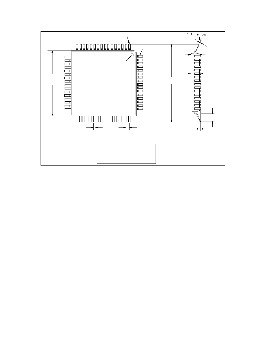
PACKAGE DETAILS
Dimensions are shown: mm (in).
FIGURE 4 ≠ LAN83C180 PACKAGE OUTLINE
10.00 (0.394)
NOM. SQ.
PIN 1 IDENT
PIN 1
PIN 64
0.17/0.27
(0.007/0.011)
64 LEADS AT
0.50 (0.020)
NOM. SPACING
12.00 (0.472)
NOM. SQ.
0 - 7
0.09/0.20
(0.004/0.008)
0.95/1.05
(0.037/0.041)
1.20 (0.047)
MAX.
0.45/0.75
(0.018/0.030)
0.05/0.15
(0.002/0.006)
64-LEAD THIN QUAD PLASTIC FLATPACK - TQFP (10 x 10 x 1.0mm)
NOTES:
1. Controlling dimensions are in millimeters.
2. This package outline diagram is for guidance
only. Please contact your local SMSC
Representative for further information.

SMSC DS ≠ LAN83C180
Page 22
Rev. 08/24/2001
LAN83C180 REVISIONS
PAGE(S)
SECTION/FIGURE/ENTRY
CORRECTION
DATE
REVISED
14
Reg 3 - LAN83C180
Identifier Register
Default value changed from 1C51h to 1C52h
08/24/01
5
Description of Pin Functions
Pin # 39 added, OSCGND - see italicized text
11/16/00
11
ICFG Interrupt
Added section
09/14/00
16
Reg. 21, Reg. 24
See Italicized Text
12/02/99
4
Pin Configuration
See Italicized Text
2/11/99
4
Figure 1
See Italicized Text
2/11/99
5, 6
Description of Pin Functions
See Italicized Text
2/11/99
10
First Paragraph under Block
Table
See Italicized Text
2/11/99
12
Transmitter Output Enable
(TXOE)
Paragraph Removed
2/11/99
18
DC Electrical
Characteristics/
DC Parameters ≠ Supply
Current
See Italicized Text
2/11/99
19
Figure 3/Pin 23
See Italicized Text
2/11/99
20
Table
See Italicized Text
2/11/99